
 admin
Microvias Can Be Used in Mixed-Signal PCBs
As electronic devices become smaller and more compact, there is a greater need for high-density interconnects (HDI). Microvias enable these connections by allowing signals and power to pass through multiple layers of the PCB. By utilizing this technology, designers can maximize space and optimize the overall performance of the device. Understanding the various types of microvias and their specific specifications is essential to leveraging this technology in your next device.
Microvias may be stacked, staggered, or a combination of both. Stacked and staggered vias can be used to minimize signal loss as well as provide room for components or traces that can’t fit on the surface of the board. Stacked and staggered vias also offer a variety of benefits to your design, including reducing the amount of copper required for the plated interface and lowering manufacturing costs.
The type of material used for the conductive filling in a microvias is critical to its electrical performance and reliability. It is important to choose a material with the appropriate properties that can handle the current load and dissipate heat effectively. It is also necessary to keep in mind the physical characteristics of the copper plating, including its thickness and texture. The substrate used to create a microvia must also be selected carefully. It must be compatible with the drilling and metallization processes and provide the necessary mechanical strength.
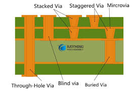
How Microvias Can Be Used in Mixed-Signal PCBs
In addition to these factors, the size and depth of a microvia is also critical to its functionality and reliability. It is recommended to use a low aspect ratio for these structures. Larger aspect ratios can cause stress concentration at the neck region, which can lead to failure under accelerated life testing or thermal cycling.
Another factor to consider when designing a microvia is the distance between the copper pad and the surrounding dielectric. This distance can impact signal transmission and can affect the impedance of a circuit. In order to minimize this effect, it is recommended to use small pad sizes and large spacing between pads.
A final factor to consider when designing a microvia structure is the aspect ratio of the hole. A microvia should be a minimum of 0.75:1 in order to meet the IPC specification. This ratio is also crucial to ensuring that the copper can be properly plated. If the hole is too large, it can prevent the copper from fully covering the entire via structure, which can lead to failure.
Microvias are an integral part of modern electronic devices. They play a vital role in enhancing signal integrity, optimizing space, and ensuring long-term reliability. Understanding the different types, their benefits, and specifications is essential to designing a high-performance PCB. By keeping up with the latest trends in microvia technology and using proper PCB layout techniques, designers can harness this advanced technology to shape future innovations.

