
 admin
primary functions of a pcb and pcba silkscreen
Printed Circuit Boards (PCBs) and Printed Circuit Board Assemblies (PCBAs) are the fundamental building blocks of electronic devices, orchestrating the seamless integration of components and facilitating the flow of electrical signals. While the intricate network of copper traces and solder joints forms the backbone of these circuitry marvels, the silkscreen layer plays a crucial supporting role, offering a host of functions aimed at enhancing functionality, manufacturability, and user experience.
At its core, the silkscreen layer of a PCB or PCBA serves as a visual aid, conveying essential information about the board’s components, orientation, and functionality. This includes markings such as component outlines, reference designators, polarity indicators, test points, and manufacturer logos. By providing clear and concise labeling, the silkscreen simplifies assembly, debugging, and maintenance processes, allowing technicians and engineers to quickly identify components and troubleshoot issues.
One of the primary functions of the silkscreen is to assist in component placement and orientation during the assembly process. By outlining the footprint of each component and indicating its orientation, polarity, and pinout, the silkscreen guides assembly technicians in accurately populating the pcb and pcba with the requisite components. This helps to minimize assembly errors and ensures that components are positioned correctly, thereby optimizing the functionality and reliability of the final product.
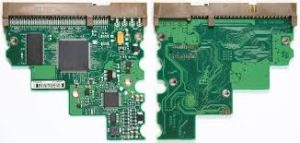
What are the primary functions of a pcb and pcba silkscreen?
Moreover, the silkscreen layer serves as a critical tool for quality control and inspection purposes. By incorporating reference designators and test points onto the PCB, the silkscreen facilitates automated testing and inspection procedures, enabling manufacturers to verify the integrity and functionality of the circuitry at various stages of the production process. This ensures that defects are identified and rectified early on, preventing costly rework and minimizing the risk of field failures.
In addition to its functional utility, the silkscreen layer also plays a significant role in enhancing the aesthetic appeal of the PCB or PCBA. Manufacturers often leverage the silkscreen layer to add branding elements such as company logos, product names, or decorative graphics, imbuing the board with a distinct identity and enhancing its visual appeal. This not only contributes to the overall professionalism and marketability of the product but also fosters brand recognition and loyalty among end-users.
Furthermore, the silkscreen layer can serve as a valuable educational tool, particularly in educational or hobbyist settings. By labeling components, pinouts, and other pertinent information, the silkscreen provides valuable insight into the inner workings of electronic circuits, helping students and enthusiasts deepen their understanding of electronics design and assembly. This educational aspect of the silkscreen layer underscores its versatility and importance beyond its primary functional roles.
Another key function of the silkscreen is to convey important safety information and compliance markings. This may include regulatory symbols, warning labels, or certification marks indicating compliance with industry standards and regulations such as RoHS (Restriction of Hazardous Substances) or CE (Conformité Européenne). By prominently displaying these markings on the PCB or PCBA, the silkscreen ensures that the product meets the necessary safety and quality requirements, instilling confidence in end-users and regulatory authorities alike.
In conclusion, the silkscreen layer of a PCB or PCBA serves a multitude of functions that are essential for its functionality, manufacturability, and user experience. From guiding component placement and aiding in inspection procedures to enhancing aesthetics and conveying important information, the silkscreen plays a pivotal role in the design, assembly, and usability of electronic devices. As technology continues to evolve, the significance of the silkscreen layer in optimizing both form and function in electronic design will undoubtedly persist.

